EasyEDA
EasyEDA - Web-based and desktop EDA suite; runs in browser, Windows, Mac, or Linux. Schematic capture, Ngspice based simulation, PCB layout, custom PCB manufacturing, fo...
- Free • Proprietary
- Circuit Simulator
- Electronic Design Automation Tool
- CAD Software
- Mac
- Windows
- Linux
- Online
What is EasyEDA?
EasyEDA is a cloud and desktop based EDA tool suite which supports open source and working collaboratively. A full suite schematic and PCB design software/manufacturing service that’s free to use and offers great prices on custom PCB manufacturing. All files in open format JSON. Can import Altium, Eagle schematics and also LTspice schematics for (limited) simulation and for conversion to PCB with full BoM support. Spice netlist import and export. Altium, PADS and Free PCB netlist export. PDF, PNG and SVG image export of all files. Users can download Gerbers and are not tied to the tool for PCB manufacture but they can buy PCBs and fully assembled PCBAs from EasyEDA if they wish.
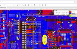
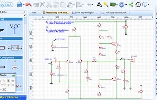
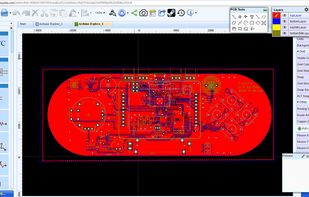
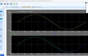
EasyEDA Screenshots


EasyEDA Features
Comments and Reviews
Tags
- eda
- Circuit Designer
- CAD
- Printed Circuit Board
- Electronics
- pcb-design
- pcb-layout
- circuit-diagram-editor
- Circuit Diagram
- Electronic Design Automation
Full circuit drawing, spice sim and board manufacturing chain. EasyEDA also offers a low cost,high quality PCB manufacturing service.
I've used it a couple of times and have been impressed by the quality of their PCBs.
Highly recommended.
[Edited by SelinaZhang2015, November 26]
Circuit Design Software On Mac :
There are many Circuit Design Softwares including different platforms ,they are based on Windows ,Linux ,or On Mac , Or based on cloud servers which you could run it anywhere .
Which tools you choose and on which platforms you choose to run was decided by your preferences , the functions you require the tools to have , the convenience of the tools , the platform you uses and so on . For most of the tools support mutil-platforms and commonly support running on windows and linux .
Let me introduce some Circuit Design Softwares that run on Mac OS .
** I. EasyEDA**
EasyEDA is Window,Linux, Mac OS and Web-Based Circuit Design Software, which supports free Schematic Capture, Spice Simulation,PCB Design .
EasyEDA provides some distinct features :
1.EasyEDA provides clean and user-friendly homepages and Editor User Interface .
enter image description here
EasyEDA Homepage
enter image description here
EasyEDA Editor UI
2.It is free and based on cloud server .
3.It supports Schematic capture ,Spice simulation,PCB Layout online .
3.It can import Schematics and PCB Files form Eagle ,Altium Designer,Kicad ,LTspice.
4.It includes abundant and increasing amount of hardware projects ,resourceful schematic libs and PCB libs created by and shared with all the EasyEDA users .
5.It supports developing with colleagues and partners collaboratively .
6.It provides easy PCB order which saves your time and effort to make sample PCB .
7.It Provides EasyEDA source file to save locally .
8.It provides SVG source to preview Schematic , PCB Layout and Gerber file .
9.EasyEDA provides rich spice models to make simulation .
10.EasyEDA provivdes simulation viewform viewer .
Design Rule Check .
There are four main functions EasyEDA provide:
1.Schematic Capture
2.Spice Simulation
3.PCB Design
4.PCB Order
enter image description here
Schematic Capture Diagram
enter image description here
Spice Simulation Waveform Viewer
enter image description here
PCB Design Tool Board .
enter image description here
PCB Order Cart
At present with the improved functions of EasyEDA , EasyEDA becomes an ideal choice for professional engineers ,students, makers, enthusiastics , hobbyists. EasyEDA provides professional online support for any EasyEDA users who has questions on using EasyEDA . EasyEDA is not only an excellent online circuit design software but also provides some favorable support and services .
More information about the tutorials of EasyEDA pls refer to
https://easyeda.com/Doc/Tutorial/
The link about the EasyEDA is as follow :
https://easyeda.com/
II.gEDA
gEDA – runs on Linux and has produced tools which are used for electrical circuit design, schematic capture, simulation, prototyping, and production. Currently, the gEDA project offers a mature suite of free software applications for electronics design, including schematic capture, attribute management, bill of materials (BOM) generation, netlisting into over 20 netlist formats, analog and digital simulation, and printed circuit board (PCB) design layout.Most gEDA applications also install and run successfully on Mac OS X, typically using the Fink package manager and Macports. Since few commercial EDA tools run on the Mac, this feature has made gEDA a popular electronic design package amongst Mac users.
The term "gEDA Suite" refers to all free software projects and applications that have associated themselves with the gEDA Project via the geda-dev/geda-user mailing lists. These include:
gEDA - gschem and friends (the original project)
PCB - PCB layout program
Gerbv - Gerber file viewer
ngspice - a port of Berkeley SPICE
GnuCap - A modern electronic circuit simulation program
gspiceui - A GUI front end for ngspice/GnuCap
gwave - An analog waveform viewer
gaw - An analog waveform viewer a rewrite of gwave. Works with gspiceui.
Icarus Verilog - A Verilog simulator
GTKWave - A digital waveform viewer
wcalc - Transmission line and electromagnetic structure analysis
enter image description here
III.McCAD
McCAD E.D.S software, a complete family of integrated electronic designs systems for MS Windows and Macintosh OS platforms. McCAD Electronic Design Systems offer a choice of design environments with a wide range of system configurations tailored to the specific needs of the designer. McCAD modules take the designer through the complete design cycle: Schematic capture, Simulation (analog & digital), Printed Circuit Board layout, Autorouting and Gerber generation for board fabrication. McCAD software gives the electronic designer the technical range needed, and at the same time provides control and flexibility.
enter image description here
IV.Osmond PCB
It is a flexible tool for designing printed circuits boards .It runs on Manintosh .Its many features include:virtually unlimited board sizes ,number of board layers,number of parts,support for both through-hole and surface mount parts and more. enter image description here
V.Macspice
MacSpice is an electronic circuit simulator. Circuit simulation is a way of building and testing virtual models of electronic devices. It is usually cheaper and quicker to simulate a design than to build a prototype. MacSpice uses a text-file 'netlist' description of the circuit as input. This is a list of components and the nodes they connect to. Users may prepare netlists with a text editor, or derive them from a circuit diagram using a third-party schematic-capture application. MacSpice then builds a numerical model of the circuit and analyses this.
MacSpice is distributed as a Mac OS X application bundle. It provides an enhanced versions of the Spice 3 simulator and the Nutmeg front-end command interpreter for data analysis and plotting. Installation notes and release notes are published on www.macpsice.com. MacSpice has several mechanisms for inter-process communication with other applications and shells.
enter image description here
VI.Qucs
Qucs is a circuit simulator with graphical user interface. The software aims to support all kinds of circuit simulation types, e.g. DC, AC, S-parameter, Transient, Noise and Harmonic Balance analysis. Pure digital simulations are also supported.
enter image description here
VII.Kicad
KiCad is a free software suite for electronic design automation (EDA). It facilitates the design of schematics for electronic circuits and their conversion to PCB designs.Tools exist within the package to create a bill of materials, artwork,Gerber files, and 3D views of the PCB and its components.
KiCad uses an integrated environment for all of the stages of the design process: Schematic Capture, PCB layout, Gerber file generation/visualization and library editing.
KiCad is cross-platform program, written with wxWidgets to run on FreeBSD, Linux, Microsoft Windows and Mac OS X. Many component libraries are available, and users can add custom components. The custom components can be available on a per-project basis, or installed for use in any project. There are also tools to help with importing components from other EDA applications, for instance EAGLE. Configuration files are in well documented plain text, which helps with interfacing to CVS's or SVN, as well as with automated component generation scripts. Up to 32 copper layers are supported.
Multiple languages are supported, such as English,Chinese,Catalan,Czech, German, Greek, Spanish, Finnish, French, Hungarian, Italian, Japanese, Korean, Dutch, Polish, Portuguese, Russian, Slovene,Swedish.
enter image description here
VIII.Eagle
Eagle is one of the most popular Circuit Design and PCB layout software available in the market. Most professionals,students and hobbyists find Eagle as an good choice for their PCB development needs. Eagle in fact is an enterprise PCB designing software but they are offering a lighter version (with limitations compared to enterprise application) for free download. CadSoft offers user friendly, powerful and affordable solutions for PCB design, including Schematic Capture, Board Layout, and Autorouter. And to your good news, Eagle will run on Windows, Linux and MAC.
There are still circuit design softwares such as DesignWorks,Osmond,Epoxy that can run on Mac . Despite this , there are still few commercial circuit design softwares based on Mac . And the above I have recommonded are some of the most popular circuit design software for Mac .Hope you enjoy the practical and wonderful circuit design software.:)
[Edited by Maple, February 29]
[Edited by Maple, February 29]
[Edited by Maple, February 29]
Circuit Design Software On Linux:
As Linux OS have become one of the most popular opensource OS for Servers and Desktop, many software will release a linux version . It also applies to the circuit design software .Since we are using the Linux as our Operationg System , and We would like to search some Circuit Design Software Based On Linux .
So let me introduce some types of Circuit design software in order to make readers more esaily choose their favorite Linux-based software .
1.EasyEDA . As a cross-platform Circuit desgin software , which is used on the browser and stored on the clound server . EasyEDA provides shematic capture , pcb layout , spice simulation and online pcb order functions which will give you an easy EDA design journey and make your circuit design work more easily and more productively . You could run it on windows , mac , linux or android platform ,as long as there is one brwoser on the OS and connecting to network.
Let me have a preview of what EasyEDA provides :
I.Schematic capture
This is a most important function of the circuit design software ,almost every circuit design software provides schematic capture function . Because it is the basic entrance of understanding the circuit you design . What is more ,it could be used to be converted into pcb design file .
Here is a screenshot of one scheamtic :
enter image description here
One Schematic—Arduino 2560 Schematic
II.Spice simulaton .
There are many spice simulation tools such as Multisim , Proteus, Ltspice , KtechLab .
EasyEDA provides many simulation models and the quick way to building models for Integrated circuits .
Also ,EasyEDA provides Waveform viewer to preview the simulation results .
enter image description here
Spice Simulation Example .
enter image description here
Spice Simulation Waveform Viewer
III.PCB layout
Almost all circuit design softwares provide PCB layout function .
This is the way to produce the PCB board and the basic tool.
EasyEDA provides laying out unlimited pads , size of the boards , and more than 6 layrers of PCB Boards.
enter image description here
PCB Layout
IV.Import from third-party EDA Tools
EasyEDA can import files from Altium Designer , LTspice ,Eagle, Kicad .
V.Export Files
EasyEDA can export EasyEDA source ,SVG source ,SVG file ,Image(png),and Pdf files.
VI.PCB Order .
EasyEDA provides online ordering PCB. When completing your Circuit PCB Design , if you do not want to spend much time on making your own PCB , you could order online PCB .
enter image description here
2.DipTrace
The second most popular software running on linux I would like to introduce is DipTrace .
DipTrace is an EDA software for designing schematic and PCB boards .
It is based on Windows ,Mac , Linux .
The Developers provide mutil-lingual interface and tutorials .
DipTrace has 4 modules: Schematic Capture Editor, PCB Layout Editor with built-in shape-based autorouter and 3D Preview & Export, Component Editor, and Pattern Editor.
There are some basic Features about DipTrace :
I.Simple UI
II.Multi-sheet and hierarchical schematics
III.High-speed shape-based autorouter
IV.Smart manual routing tools
V.Wide import / export capabilities
VI.Advanced verifications with real-time DRC
VII.Real-time 3D PCB preview & STEP export
VIII.Manufacturing output
There are five modules for DipTrace .
enter image description here
Schematic Capture
enter image description here
PCB Layout
enter image description here
3D Preview and Export
enter image description here
Component Editor
enter image description here
Pattern Editor
3.gEDA
gEDA is so important for it is firstly started in an effort to remedy the lack of free software EDA for Linux/Unix . And one of the long standing goal for gEDA is to provide a suite od EDA application for Linux .
All applications in the gEDA suite compile and run on Linux. So it is the software that I could not miss on introducing circuit design software on Linux.
There are three main features gEDA provides:
I.gEDA provides schematic capture :
enter image description here
II.gEDA provides PCB Editor
enter image description here
III.gerber file viewer
enter image description here
Here I should have to mention the term “gEDA Suite”.
The term“gEDA”refers to all free software projects and applications that have asscioated with the gEDA project .
These include:
· gEDA/gaf - gschem and friends (the original project)
· PCB - PCB layout program
· Gerbv - Gerber file viewer
· ngspice - a port of Berkeley SPICE
· GnuCap - A modern electronic circuit simulation program
· gspiceui - A GUI front end for ngspice/GnuCap
· gwave - An analog waveform viewer
· gaw - An analog waveform viewer a rewrite of gwave. Works with gspiceui.
· Icarus Verilog - A Verilog simulator
· GTKWave - A digital waveform viewer
· wcalc - Transmission line and electromagnetic structure analysis
For the importance of Linux to electronic design ,the open-source developers recognize it many years ago , and the gEDA is the proof of their early insight .
The gEDA Project remains a federation of software tools developed by different (but sometimes overlapping) programmers.
The thread which holds the project together is the shared vision of creating a powerful, community-based, open-source EDA toolkit.
4.Qucs Quite Universal Circuit Simulator (Qucs) is an open-source electronic circuit simulator software release under the GPL .
It give you the ability to setup a circuit with graphical user interface and simulate the large-signal, small-signal and noise behaviour of the circuit.
Qucs supports a growing list of analog and digital components as well as SPICE sub-circuits. It is intended to be much simpler to use and handle than other circuit simulators like gEDA or PSPICE.
enter image description here
5.Magic
Now let me introduce a very-large-integration layout tool originally written by John Ousterhout his graduate students at UC Berkeley during the 1980s.
As a free and opensource software ,subject to the requirement of BSD Licence ,Magic continues to be popular because it is easy to use and easy to expand for specialized tasks .
Magic is widely cited as being the easiest tool to use for circuit layout, even for people who ultimately rely on commercial tools for their product design flow.
enter image description here
So far I have recommend several circuit design tools on Linux .
There are also Kicad ,eagle ,Fritzing,Open Circuit Design, and some other kinds of software that can run on Linux .
As for the restriction of article length, Here I do not list all the circuit design software with detailed descriptions .
Hope you could enjoy the free and all-platform supported tools like Easyeda, the linux-originated software tool like gEDA, the very-large-integration layout tool like Magic etc .
Circuit simulator and PCB design software - EasyEDA EasyEDA is a free, zero- install, cloud-based EDA tool, designed to give electrical engineers, educators, engineering students and electronics hobbyists an Easier EDA Experience. It is easy to use circuit design, circuit simulator and PCB design that runs in your web browser. Features of EasyEDA: Cool Schematic Capture Draw schematics quickly using the available libraries on browser. Seamless automatic upgrades. Circuit Simulator Verify analog, digital and mixed signal circuits with spice subcircuits and models! Online PCB Design With multiple layers, thousands of pads, you could still operate quickly and layout smoothly. The system is very stable, reliable and easy to learn. The user interface is very pleasant and responsive operation.EasyEDA has a rich library of thousands of electronic components (for both circuits and printed circuit boards, and for modeling), and tens of thousands of examples of schematics! Anyone can use this library and expand it. It also can import existing designs done in Altium, Eagle and KiCad and then edit them in EasyEDA . Moreover, another outstanding feature of EasyEDA is that users can access to Open Source modules developed by thousands of electronics engineers. There is a tutorial explaining the main features of the tool and a Simulation ebook, introducing circuit simulation in EasyEDA using ngspice. easyeda.com
How to Make PCB on Easyeda ?
1.What is PCB ? A printed circuit board (PCB) mechanically supports and electrically connects electronic components using conductive tracks, pads and other features etched from copper sheets laminated onto a non-conductive substrate.
PCBs can be single sided (one copper layer), double sided (two copper layers) or multi-layer (outer and inner layers).
Multi-layer PCBs allow for much higher component density. Conductors on different layers are connected with plated-through holes called vias.
Advanced PCBs may contain components - capacitors, resistors or active devices - embedded in the substrate.
2.The Process of Making a PCB Board ?
I.Start with a schematic
II.Layout PCB
III.Convert PCB File to Gerber File
IV.Send to PCB Factory for sample production
1.Design Schematic , on Easyeda , for example , design an Atmega16 simpliest system .
1.1.Create a Project . Document -New -Project
1.2.Create a Schematic and start designig a simplest system of MCU .
enter image description here
2.Make a PCB
2.1.Convert schematic to PCB and then Place the components in the proper position inside the Mechanical framework : enter image description here
2.2.Start Routing a PCB manually .
2.2.1.Tips to Make PCB Circuit Board:
Sizing Traces Real-world copper traces have resistance. This means that a trace has a voltage drop, power dissipation, and a temperature rise when current flows through it. Resistance is defined by this formula: R=(resistivitylength)(thicknesswidth) PCB designers most commonly use length, thickness, and width to control the resistance of a PCB trace. Resistance is a physical property of the metal used to make the trace. PCB designers can't really change the physical properties of copper, so focus on the trace size, which you can control. PCB trace thickness is measured in ounces of copper. One ounce of copper is the thickness we would measure if we evenly spread 1 oz of copper over a 1 square foot area. This thickness is 1.4 thousandths of an inch. Many PCB designers use 1 oz or 2 oz copper, but many PCB manufacturers can provide 6 oz thickness. Note that fine features like pins that are close together are hard to make in thick copper. Consult your PCB manufacturer about what their capabilities are. Use a PCB trace width calculator to determine how thick and wide your traces should be for your application. Aim for a 5°C temperature rise. If you have extra space on the board, use bigger traces, as they don’t cost anything. When doing a multi-layer board, remember that traces on external layers have better cooling than traces on internal layers because the heat from inner layers has to travel through layers of copper and PCB material before being conducted, radiated, or connected away. Make Loops Small Loops, especially high frequency loops, should be made as small as possible. Small loops have lower inductance and resistance. Placing loops over a ground plane further reduces inductance. Having small loops reduces high frequency voltage spikes caused by V=Ldidt . Small loops also help reduce the amount of signals that are inductively coupled into the node from external sources, or are broadcast from the node. This is what you want, unless you’re designing an antenna. Also keep loops small for op-amp circuits to prevent noise from being coupled into the circuit. Decoupling Capacitor Placement Place decoupling capacitors as near as possible to the power and ground pins of integrated circuits to maximize decoupling efficiency. Placing capacitors farther away introduces stray inductance. Multiple vias from the capacitor's pin to a ground plane reduce inductance.
Kelving Connections
Kelvin connections are useful for measurements. Kelvin connections are made at the exact points to reduce stray resistance and inductance. For example, Kelvin connections for a current sense resistor are placed exactly at the resistor pads, not at some arbitrary place on the traces. Although on the schematic, placing the connections at the resistor pads or at some arbitrary point may look the same, real traces have inductance and resistance that could throw your measurements off if you don’t use. Keep Digital and Noisy Traces Away from Analog Traces Parallel traces or conductors form a capacitor. Placing traces close together capacitively couples the signals on the traces, especially if the signals are high frequency. Keep high frequency and noisy traces away from traces that you don’t want noise on. Ground is not ground Ground is not an ideal conductor. Take care to route noisy grounds away from signals that need to be quiet. Make ground traces large enough to carry the currents that will flow. Placing a ground plane directly under signal traces lowers the impedance of the traces, which is ideal. Via Size and number
Vias have inductance and resistance. If you’re routing a trace from one side of the PCB to the other and need low inductance or resistance, use multiple vias. Large vias have lower resistance. This is especially useful in grounding filter capacitors and high current nodes.
Thermal vias
Vias can be used to move heat from one side of a PCB to the other. This is especially useful when a PCB is mounted on a heatsink on a chassis that can further dissipate heat. Large vias transfer heat more efficiently than small vias. Many vias transfer heat more efficiently than one via, and lower the operating temperature of components. Lower operating temperatures contribute to higher reliability. Distances between traces and mouting holes. Leave room between copper traces or fills and mounting holes; this helps prevent shock hazards. Solder mask isn’t considered a reliable insulator, so take care that there is distance between copper and any mounting hardware.
Heat sensitive components
Keep components that are sensitive to heat away from other components that generate heat. Examples of components that are sensitive to heat include thermocouples and electrolytic capacitors. Placing thermocouples close to heat sources may throw off temperature measurements. Placing electrolytic capacitors close to heat generating components will reduce their operating life. Components that generate heat may include bridge rectifiers, diodes, MOSFETs, inductors, and resistors. The heat depends on current flowing through the components.
Width of Trace :
The minimum width of trace is 4 mil when you layout very simple circuits ,and when you layout the current traces , you need to consider the width of Traces. Here with the relationship between the Trace width and the current . Copper Thickness
35UM 50UM 70UM
Width Current Width Current Width Current
0.15 0.20 0.15 0.50 0.15 0.70
0.20 0.55 0.20 0.70 0.20 0.90
0.30 0.80 0.30 1.10 0.30 1.30
0.40 1.10 0.40 1.35 0.40 1.70
0.50 1.35 0.50 1.70 0.50 2.00
0.60 1.60 0.60 1.90 0.60 2.30
0.80 2.00 0.80 2.40 0.80 2.80
1.00 2.30 1.00 2.60 1.00 3.20
1.20 2.70 1.20 3.00 1.20 3.60
1.50 3.20 1.50 3.50 1.50 4.20
2.00 4.00 2.00 4.30 2.00 5.10
2.50 4.50 2.50 5.10 2.50 6.00
Laying out DC-DC voltage Circuits
Laying out a DC-DC circuits , it should obey very strict rules according to the DC-DC Converter Datasheet .
Laying out High Speed Circuits and differential Circuits
Laying out High-speed circuits also require designers to consider its impedance matching .And for the differential circuits we should parallel the wires and make impedance matching through a GND Layer or Power Layer. Every High-Frequency circuits requires impedance matching should be provided with a referential Layer .
Keep Noisy Circuits away from High-Speed Circuits
Noisy circuits too close to High-Speed circuits may cause the the High-Speed singal to distortion and affect normal operation of High-Speed circuits .
2.2.2.The Result of the MCU PCB Layout . enter image description here 2.2.3.Pour the Copper on the BottomLayer . enter image description here https://easyeda.com/GerryChen/MCU_Project-HFzQ82kCU 3.Click the Photo view to check the Gerber file enter image description here 4.Send Gerber file to PCB factory for PCB production and debug the the circuits by welding the components and ICs . That is a complete process of Making PCB board and Testing ?Debuging the circuits . 5. Easyeda Provides an cheap PCB Cart which offers low-price PCB and improve your efficiency to Make PCB . Easyeda provides an Fabrication Output function . By clicking it , You can add the pcb order to cart and order the pcb board . You could wait at home or your company for the PCB and weld components at home or send to be welded by factory ,especially ICs with BGA Package . Easyeda provides a one-stop shop for Electronics projects .You could go to it and experience designing Schematic & PCB and order PCB. https://easyeda.com/
[Edited by Maple, February 22]
Circuit simulator and PCB design software - EasyEDA
EasyEDA is a free, zero- install, cloud-based EDA tool, designed to give electrical engineers, educators, engineering students and electronics hobbyists an Easier EDA Experience. It is easy to use circuit design, circuit simulator and PCB design that runs in your web browser. Features of EasyEDA: Cool Schematic Capture Draw schematics quickly using the available libraries on browser. Seamless automatic upgrades. Circuit Simulator Verify analog, digital and mixed signal circuits with spice subcircuits and models! Online PCB Design With multiple layers, thousands of pads, you could still operate quickly and layout smoothly. The system is very stable, reliable and easy to learn. The user interface is very pleasant and responsive operation.EasyEDA has a rich library of thousands of electronic components (for both circuits and printed circuit boards, and for modeling), and tens of thousands of examples of schematics! Anyone can use this library and expand it. It also can import existing designs done in Altium, Eagle and KiCad and then edit them in EasyEDA . Moreover, another outstanding feature of EasyEDA is that users can access to Open Source modules developed by thousands of electronics engineers.
There is a tutorial explaining the main features of the tool and a Simulation ebook, introducing circuit simulation in EasyEDA using ngspice. The following video briefly presents the features of EasyEDA tool.
https://easyeda.com/