
JumboCAD EDA
1 like
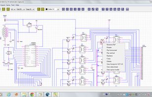
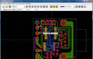
JumboCAD EDA contains 3 packages, Schematic Capture, PCB designer and Library Editor.
Cost / License
- Free
- Proprietary
Platforms
- Windows
Features
No features, maybe you want to suggest one?
JumboCAD EDA News & Activities
Highlights All activities
Recent activities
No activities found.
JumboCAD EDA information
No comments or reviews, maybe you want to be first?
What is JumboCAD EDA?
- Schematic Capture
- Easy to use, place parts, move parts, place wires only simply by moving and dragging your mouse. Use mouse wheel to zoom in and zoom out.
- Simple hot-keys. CTRL-C (copy), CTRL-Z (Undo), delete (delete), F1 (Toggle pan mode), CTRL-W (draw wire), CTRL-R (rotate). No other hot-key
- Support PAN mode. Use "F1" or mouse wheel to zoom in and zoom out.
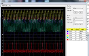
- Use XYCE as circuit simulator engine.
- BOM generation, PCB netlist generation
- Auto annotate
- PCB designer -Easy to use. Place parts, move parts, draw traces simply by moving and dragging your mouse. Zoom in & out by mouse wheel.
- Simple hot keys, CTRL-C (copy), CTRL-Z (Undo), delete (delete), F1 (Toggle pan mode), CTRL-R (rotate). No other hot-key
- Support PAN mode. Use "F1" or mouse wheel to zoom in and out.
- Support Unit in "mil" or "mm. Snap value can be any value. Precision up to 3 decimal place for "mm", 1 decial place for "mil"
- Includes find part, find net, hight current net features.
- support netlist import and re-import. User can re-generate the PCB netlist to reflect the changes of schematic.
- Gerber files,design rule check (DRC).
- Work up to 16 conductive layers (Inner1-Inner13 are for evaluation purpose only, they are not yet tested)


